1
Data sheet acquired from Harris Semiconductor
SCHS207
Features
∑ Onboard Oscillator
∑ Common Reset
∑ Negative Edge Clocking
∑ Typical f
MAX
= 50MHz at V
CC
= 5V, C
L
= 15pF,
T
A
= 25
o
C
∑ Fanout (Over Temperature Range)
- Standard Outputs . . . . . . . . . . . . . . . 10 LSTTL Loads
- Bus Driver Outputs . . . . . . . . . . . . . 15 LSTTL Loads
∑ Wide Operating Temperature Range . . . -55
o
C to 125
o
C
∑ Balanced Propagation Delay and Transition Times
∑ Significant Power Reduction Compared to LSTTL
Logic ICs
∑ HC Types
- 2V to 6V Operation
- High Noise Immunity: N
IL
= 30%, N
IH
= 30% of V
CC
at V
CC
= 5V
∑ HCT Types
- 4.5V to 5.5V Operation
- Direct LSTTL Input Logic Compatibility,
V
IL
= 0.8V (Max), V
IH
= 2V (Min)
- CMOS Input Compatibility, I
l
1
µ
A at V
OL
, V
OH
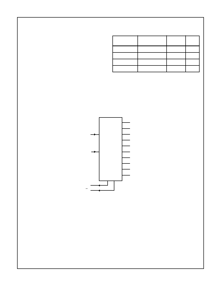
Pinout
CD74HC4060, CD74HCT4060
(PDIP, SOIC)
TOP VIEW
14
15
16
9
13
12
11
10
1
2
3
4
5
7
6
8
Q12
Q13
Q14
Q6
Q5
Q7
GND
Q4
V
CC
Q8
Q9
MR
I
O
O
Q10
February 1998
CAUTION: These devices are sensitive to electrostatic discharge. Users should follow proper IC Handling Procedures.
Copyright
©
Harris Corporation 1998
File Number
1654.1
CD74HC4060,
CD74HCT4060
High Speed CMOS Logic
14-Stage Binary Counter with Oscillator
[ /Title
(CD74
HC406
0,
CD74
HCT40
60)
/Sub-
ject
(High
Speed
CMOS
2
Description
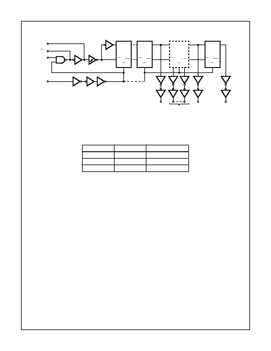
The Harris CD74HC4060 and CD74HCT4060 each consist
of an oscillator section and 14 ripple-carry binary counter
stages. The oscillator configuration allows design of either
RC or crystal oscillator circuits. A Master Reset input is
provided which resets the counter to the all-0's state and
disables the oscillator. A high level on the MR line
accomplishes the reset function. All counter stages are
master-slave flip-flops. The state of the counter is advanced
one step in binary order on the negative transition of
I (and
O). All inputs and outputs are buffered. Schmitt trigger
action on the input-pulse-line permits unlimited rise and fall
times.
In order to achieve a symmetrical waveform in the oscillator
section the HCT4060 input pulse switch points are the same
as in the HC4060; only the MR input in the HCT4060 has
TTL switching levels.
Functional Diagram
Ordering Information
PART NUMBER
TEMP. RANGE (
o
C)
PACKAGE
PKG.
NO.
CD74HC4060E
-55 to 125
16 Ld PDIP
E16.3
CD74HCT4060E
-55 to 125
16 Ld PDIP
E16.3
CD74HC4060M
-55 to 125
16 Ld SOIC
M16.15
CD74HCT4060M
-55 to 125
16 Ld SOIC
M16.15
NOTES:
1. When ordering, use the entire part number. Add the suffix 96 to
obtain the variant in the tape and reel.
2. Wafer and die for this part number is available which meets all
electrical specifications. Please contact your local sales office or
Harris customer service for ordering information.
I
Q4
Q5
Q6
Q7
Q9
Q12
Q14
O
O
MR
Q13
Q10
Q8
14-STAGE
RIPPLE
COUNTER
AND
OSCILLATOR
GND = 8
V
CC
= 16
7
5
4
6
13
1
3
2
15
14
12
11
9
10
CD74HC4060, CD74HCT4060
4
Absolute Maximum Ratings
Thermal Information
DC Supply Voltage, V
CC
. . . . . . . . . . . . . . . . . . . . . . . . -0.5V to 7V
DC Input Diode Current, I
IK
For V
I
< -0.5V or V
I
> V
CC
+ 0.5V
. . . . . . . . . . . . . . . . . . . . . .±
20mA
DC Output Diode Current, I
OK
For V
O
< -0.5V or V
O
> V
CC
+ 0.5V
. . . . . . . . . . . . . . . . . . . .±
20mA
DC Drain Current, per Output, I
O
For -0.5V < V
O
< V
CC
+ 0.5V
. . . . . . . . . . . . . . . . . . . . . . . . . .±
25mA
DC V
CC
or Ground Current, I
CC
. . . . . . . . . . . . . . . . . . . . . . . . .±
50mA
Operating Conditions
Temperature Range, T
A
. . . . . . . . . . . . . . . . . . . . . . -55
o
C to 125
o
C
Supply Voltage Range, V
CC
HC Types . . . . . . . . . . . . . . . . . . . . . . . . . . . . . . . . . . . . .2V to 6V
HCT Types . . . . . . . . . . . . . . . . . . . . . . . . . . . . . . . . .4.5V to 5.5V
DC Input or Output Voltage, V
I
, V
O
. . . . . . . . . . . . . . . . . 0V to V
CC
Input Rise and Fall Time
2V . . . . . . . . . . . . . . . . . . . . . . . . . . . . . . . . . . . . . . 1000ns (Max)
4.5V. . . . . . . . . . . . . . . . . . . . . . . . . . . . . . . . . . . . . . 500ns (Max)
6V . . . . . . . . . . . . . . . . . . . . . . . . . . . . . . . . . . . . . . . 400ns (Max)
Thermal Resistance (Typical, Note 3)
JA
(
o
C/W)
PDIP Package . . . . . . . . . . . . . . . . . . . . . . . . . . . . .
90
SOIC Package . . . . . . . . . . . . . . . . . . . . . . . . . . . . .
160
Maximum Junction Temperature . . . . . . . . . . . . . . . . . . . . . . . 150
o
C
Maximum Storage Temperature Range . . . . . . . . . .-65
o
C to 150
o
C
Maximum Lead Temperature (Soldering 10s) . . . . . . . . . . . . . 300
o
C
(SOIC - Lead Tips Only)
CAUTION: Stresses above those listed in "Absolute Maximum Ratings" may cause permanent damage to the device. This is a stress only rating and operation
of the device at these or any other conditions above those indicated in the operational sections of this specification is not implied.
NOTE:
3.
JA
is measured with the component mounted on an evaluation PC board in free air.
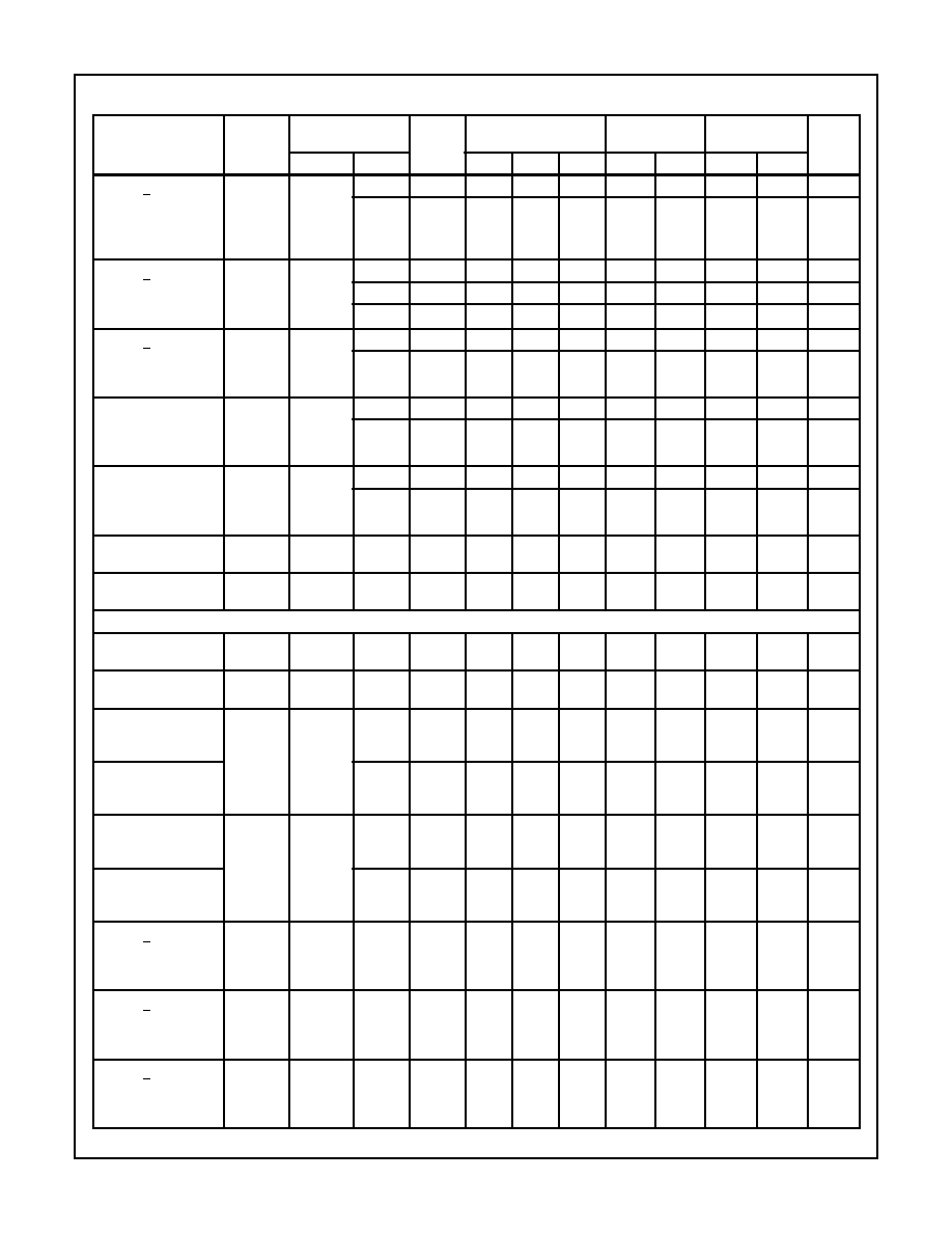
DC Electrical Specifications
PARAMETER
SYMBOL
TEST
CONDITIONS
V
CC
(V)
25
o
C
-40
o
C TO 85
o
C -55
o
C TO 125
o
C
UNITS
V
I
(V)
I
O
(mA)
MIN
TYP
MAX
MIN
MAX
MIN
MAX
HC TYPES
High Level Input
Voltage
V
IH
-
-
2
1.5
-
-
1.5
-
1.5
-
V
4.5
3.15
-
-
3.15
-
3.15
-
V
6
4.2
-
-
4.2
-
4.2
-
V
Low Level Input
Voltage
V
IL
-
-
2
-
-
0.5
-
0.5
-
0.5
V
4.5
-
-
1.35
-
1.35
-
1.35
V
6
-
-
1.8
-
1.8
-
1.8
V
High Level Output
Voltage Q Outputs
CMOS Loads
V
OH
V
IH
or V
IL
-0.02
2
1.9
-
-
1.9
-
1.9
-
V
-0.02
4.5
4.4
-
-
4.4
-
4.4
-
V
-0.02
6
5.9
-
-
5.9
-
5.9
-
V
High Level Output
Voltage Q Outputs
TTL Loads
-
-
-
-
-
-
-
-
-
V
-4
4.5
3.98
-
-
3.84
-
3.7
-
V
-5.2
6
5.48
-
-
5.34
-
5.2
-
V
Low Level Output
Voltage Q Outputs
CMOS Loads
V
OL
V
IH
or V
IL
0.02
2
-
-
0.1
-
0.1
-
0.1
V
0.02
4.5
-
-
0.1
-
0.1
-
0.1
V
0.02
6
-
-
0.1
-
0.1
-
0.1
V
Low Level Output
Voltage Q Outputs
TTL Loads
-
-
-
-
-
-
-
-
-
V
4
4.5
-
-
0.26
-
0.33
-
0.4
V
5.2
6
-
-
0.26
-
0.33
-
0.4
V
High-Level Output
Voltage
O Output
(Pin 10)
CMOS Loads
V
OH
V
CC
or
GND
-0.02
2
1.9
-
-
1.9
-
1.9
-
V
-0.02
4.5
4.4
-
-
4.4
-
4.4
-
V
-0.02
6
5.9
-
-
5.9
-
5.9
-
V
CD74HC4060, CD74HCT4060
5
High-Level Output
Voltage
O Output
(Pin 10)
TTL Loads
Note 6
V
OH
V
CC
or
GND
-2.6
4.5
3.98
-
-
3.84
-
3.7
-
V
-3.3
6
5.48
-
-
5.34
-
5.2
-
V
Low-Level Output
Voltage
O Output
(Pin 10)
CMOS Loads
V
OL
V
CC
or
GND
0.02
2
-
-
0.1
-
0.1
-
0.1
V
0.02
4.5
-
-
0.1
-
0.1
-
0.1
V
0.02
6
-
-
0.1
-
0.1
-
0.1
V
Low-Level Output
Voltage
O Output
(Pin 10)
TTL Loads
V
OL
V
CC
or
GND
2.6
4.5
-
-
0.26
-
0.33
-
0.4
V
3.3
6
-
-
0.26
-
0.33
-
0.4
V
High-Level Output
Voltage
O Output
(Pin 9)
TTL Loads
V
OH
V
IL
or V
IH
-3.2
4.5
3.98
-
-
3.84
-
3.7
-
V
-4.2
6
5.48
-
-
5.34
-
5.2
-
V
Low-Level Output
Voltage
O Output
(Pin 9)
TTL Loads
V
OL
V
IL
or V
IH
-2.6
4.5
-
-
0.26
-
0.33
-
0.4
V
-3.3
6
-
-
0.26
-
0.33
-
0.4
V
Input Leakage
Current
I
I
V
CC
or
GND
-
6
-
-
±
0.1
-
±
1
-
±
1
µ
A
Quiescent Device
Current
I
CC
V
CC
or
GND
0
6
-
-
8
-
80
-
160
µ
A
HCT TYPES
High Level Input
Voltage
V
IH
-
-
4.5 to
5.5
2
-
-
2
-
2
-
V
Low Level Input
Voltage
V
IL
-
-
4.5 to
5.5
-
-
0.8
-
0.8
-
0.8
V
High Level Output
Voltage Q Outputs
CMOS Loads
V
OH
V
IH
or V
IL
Note 5
-0.02
4.5
4.4
-
-
4.4
-
4.4
-
V
High Level Output
Voltage Q Outputs
TTL Loads
-4
4.5
3.98
-
-
3.84
-
3.7
-
V
Low Level Output
Voltage Q Outputs
CMOS Loads
V
OL
V
IH
or V
IL
Note 5
0.02
4.5
-
-
0.1
-
0.1
-
0.1
V
Low Level Output
Voltage Q Outputs
TTL Loads
4
4.5
-
-
0.26
-
0.33
-
0.4
V
High-Level Output
Voltage
O Output
(Pin 10)
CMOS Loads
V
OH
V
CC
or
GND
-0.02
4.5
4.4
-
-
4.4
-
4.4
-
V
High-Level Output
Voltage
O Output
(Pin 10)
TTL Loads Note 6
V
OH
V
CC
or
GND
-2.6
4.5
3.98
-
-
3.84
-
3.7
-
V
Low-Level Output
Voltage
O Output
(Pin 10)
CMOS Loads
V
OL
V
CC
or
GND
0.02
4.5
-
-
0.1
-
0.1
-
0.1
V
DC Electrical Specifications
(Continued)
PARAMETER
SYMBOL
TEST
CONDITIONS
V
CC
(V)
25
o
C
-40
o
C TO 85
o
C -55
o
C TO 125
o
C
UNITS
V
I
(V)
I
O
(mA)
MIN
TYP
MAX
MIN
MAX
MIN
MAX
CD74HC4060, CD74HCT4060